Polysilicon And Wafer Supply Chain
Origin and history
The polysilicon and wafer supply chain originates from the semiconductor industry, which began its modern development in the mid-20th century in the United States. The foundational process for producing high-purity polysilicon, known as the Siemens process, was commercialized in Germany during the 1950s. This supply chain evolved separately for the electronics and solar industries, with the solar photovoltaic (PV) sector becoming a major driver from the late 1990s onward. Initial production was concentrated in the United States, Europe, and Japan before undergoing massive geographical shifts. The early 2000s saw the rise of Chinese manufacturers who entered the polysilicon market, later expanding into wafer production. Today, the supply chain is a globally interconnected network, though its center of mass for manufacturing has moved decisively to East Asia.
What it is for
This supply chain exists to transform raw quartzite into the ultra-pure, crystalline silicon substrates essential for manufacturing semiconductor devices. Its primary output is the silicon wafer, a thin, polished disc that serves as the foundational physical platform for integrated circuits. For the solar energy industry, the chain produces slightly less pure polysilicon that is crystallized into ingots and sliced into thinner wafers for photovoltaic cells. The entire sequence is engineered to achieve and preserve extreme levels of material purity, measured in parts per billion for electronic-grade silicon. It provides the basic building material without which modern computing, telecommunications, and renewable energy generation would not exist. The specifications for wafers, including diameter, crystal structure, and surface perfection, are dictated by the downstream fabrication processes of chipmakers and solar cell producers.
Overview
The polysilicon and wafer supply chain is a multi-stage, capital-intensive industrial process involving distinct specialized companies. It begins with the mining and refining of quartzite to produce metallurgical-grade silicon, a material of about 98% purity. This is then chemically purified via the Siemens process or fluidized bed reactor (FBR) method to produce electronic-grade or solar-grade polysilicon, which is a high-purity, granular or rod-shaped form. The polysilicon is then melted in a crucible and grown into a single crystal structure, either through the Czochralski (CZ) method for most electronics or the directional solidification method for solar, creating cylindrical ingots. These ingots are then trimmed, sized, and sliced into thin wafers using wire saws, a process that generates significant material loss as kerf. The wafers subsequently undergo edge grinding, lapping, etching, and polishing to achieve the required mechanical, chemical, and surface properties before shipment to chip or cell fabs.
What to know
The supply chain is characterized by extreme economies of scale and high barriers to entry due to enormous capital requirements and complex, proprietary technology. Geopolitical factors are critically important, as production is heavily concentrated in specific regions, creating vulnerabilities and trade tensions, particularly between China and other nations. Polysilicon production is highly energy-intensive, making electricity cost and carbon footprint major factors in facility location and product competitiveness. There is a fundamental technological divergence between the tighter purity requirements for semiconductor wafers and the cost-driven production for solar wafers, though some processes overlap. The industry is cyclical, prone to periods of overcapacity and shortages driven by mismatches between capital investment lag times and demand fluctuations in downstream electronics and solar markets. Continuous innovation focuses on increasing wafer sizes, reducing kerf loss during slicing, and improving crystal growth efficiency to lower costs.
Common questions
What is the difference between polysilicon and a silicon wafer? Polysilicon is the high-purity raw material, while a wafer is the finished, polished slice of single-crystal silicon made from melted and recrystallized polysilicon. Why is China dominant in this supply chain? China achieved dominance through aggressive government-backed investment, lower energy and labor costs, and vertical integration, capturing over 80% of the global capacity across multiple stages. Can solar-grade polysilicon be used for semiconductors? Generally no, as solar-grade silicon has higher tolerance for certain impurities that would ruin the performance of electronic microchips. How are wafer sizes standardized? The industry has moved through generations, from 100mm to 300mm and now 450mm for electronics, driven by the need for more chips per wafer to improve economics. What happens to the silicon dust from wafer sawing? This kerf loss, which can account for up to 40% of the ingot, is often recycled back into the process after cleaning or used in other industries like metallurgy. Is there an alternative to silicon wafers? For mainstream computing and solar, no; silicon's abundance, stability, and well-understood properties make it irreplaceable, though compound semiconductors like gallium arsenide serve niche applications.
Pros and cons
The deep specialization and vertical integration of leading players create efficiency and drive relentless technological improvement in wafer size and quality. However, the extreme concentration of production in one geographical region creates profound supply chain risk, where trade disputes or regional disruptions can cripple global industries. The capital intensity leads to boom-bust cycles where companies often over-expand during periods of high demand, leading to destructive price wars and bankruptcies when demand growth temporarily slows. A common regret for new entrants is underestimating the complexity of scaling production while maintaining consistent purity and yield, often resulting in massive financial losses. The environmental footprint, particularly the high energy consumption and hazardous chemical byproducts of polysilicon purification, remains a significant and costly challenge to mitigate, attracting regulatory scrutiny.
Who it suits
This supply chain suits large, well-capitalized corporations and nations with access to cheap, reliable energy and strong government support for strategic industries. It is ideal for vertically integrated companies that can control multiple stages, from polysilicon to cells or chips, to secure margins and ensure quality control. The semiconductor-grade segment suits firms with decades of metallurgical and chemical engineering expertise, capable of operating in a high-precision, lower-volume environment. The solar-grade segment is suited for producers focused intensely on scale, operational efficiency, and incremental process innovation to shave costs. It does not suit small players or startups without billions in capital and years of technical ramp-up time. End-users, like solar project developers, are increasingly suited to those with secure, diversified supplier relationships or long-term contracts to navigate the market's volatility and supply constraints.
Latest Polysilicon And Wafer Supply Chain news
Latest reporting
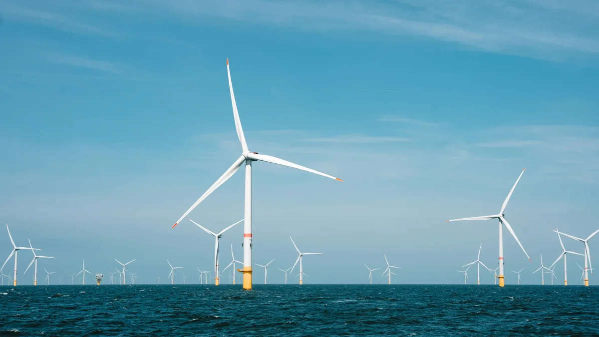
Tekmar secures €6 million offshore wind
Tekmar Group has won a €6 million contract extension to supply cable protection systems for a European offshore wind project, with manufacturing set...
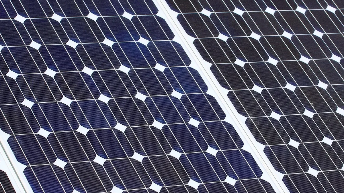
India's Solar Manufacturing Surge Faces Cell Supply
India added 50.6GW of solar module and 9.7GW of cell capacity in H1 2026, but a critical shortage of domestic cells is slowing production and project
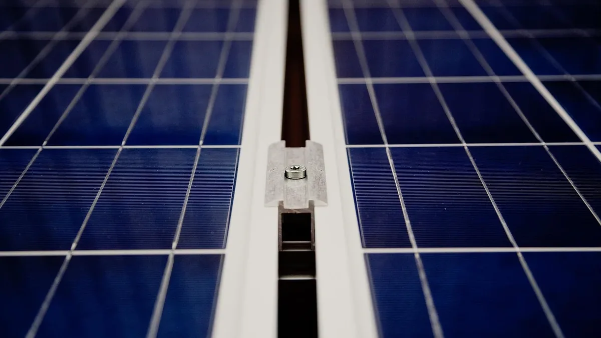
Section 232 tariff drives solar module prices up over 40%
A new 15% tariff on polysilicon imports, effective December 4, has already pushed median U.S. solar module prices from $0.27/W to $0.38/W.
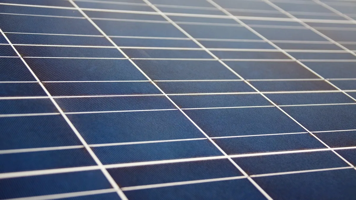
Gray vs. Blue wafer distinction critical for U.S. Solar
The technical difference between unprocessed gray wafers and partially finished blue wafers is central to accurately assessing domestic manufacturing...
PJM Proposes 6GW Auction to Cover Data Centre Power
Grid operator PJM has submitted a two-part plan to FERC, proposing a one-time 6GW capacity auction and shifting responsibility for new supply to large
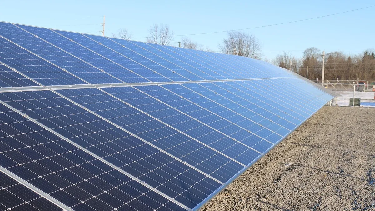
Inox Solar Americas signs 767MW US module
Inox Solar Americas has agreed to supply 767MW of solar modules for three utility-scale projects in North Carolina and Texas, with deliveries...