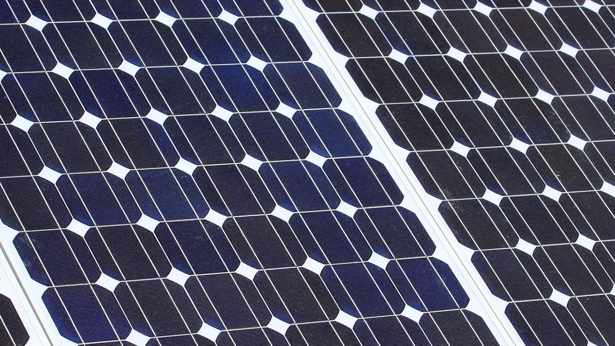
Back Contact Cells
| Generation technology | Third-generation photovoltaics |
|---|---|
| Specific project | RECALL (Research on Advanced Back-Contact Cells and Modules) |
| First created | 1990s (decade precision) |
| Original use | High-efficiency solar power generation |
| Key structural feature | All electrical contacts on rear cell surface |
| Primary advantage | Increased light capture on front surface |
| Typical efficiency class | High (laboratory cells exceed 25%) |
Origin and history
Back contact solar cell technology originated from research and development efforts in the United States and Europe during the late 20th century. The core concept was first seriously investigated and documented in the 1970s as researchers sought methods to reduce shading losses from front-side metal contacts. Significant development milestones were achieved in the 1990s, particularly with the work on point-contact cells at Stanford University. These early point-contact designs demonstrated the high-efficiency potential of moving all electrical contacts to the rear of the silicon wafer. Parallel development occurred in Europe, with research institutions and companies exploring interdigitated back contact (IBC) architectures. The technology transitioned from laboratory prototypes to commercial pilot lines in the first decade of the 21st century, establishing its industrial viability.
What it is for
This technology is for converting sunlight into electricity with maximum efficiency and improved aesthetics in photovoltaic modules. Its primary purpose is to eliminate optical losses caused by the shadowing of front-side metal grid lines, which block light from reaching the semiconductor. By moving all contacts to the rear, it allows the entire front surface to be used for light absorption without obstruction. This design is particularly suited for applications where high energy yield per unit area is critical, such as on rooftops with limited space or in utility-scale solar parks aiming to maximize land use. Furthermore, the uniform black appearance of the cells makes them desirable for architectural integration and consumer-facing products where visual appeal is a factor. The technology also aims to reduce electrical losses by enabling optimized, low-resistance contact patterns that are not constrained by the need for light transmission.
Overview
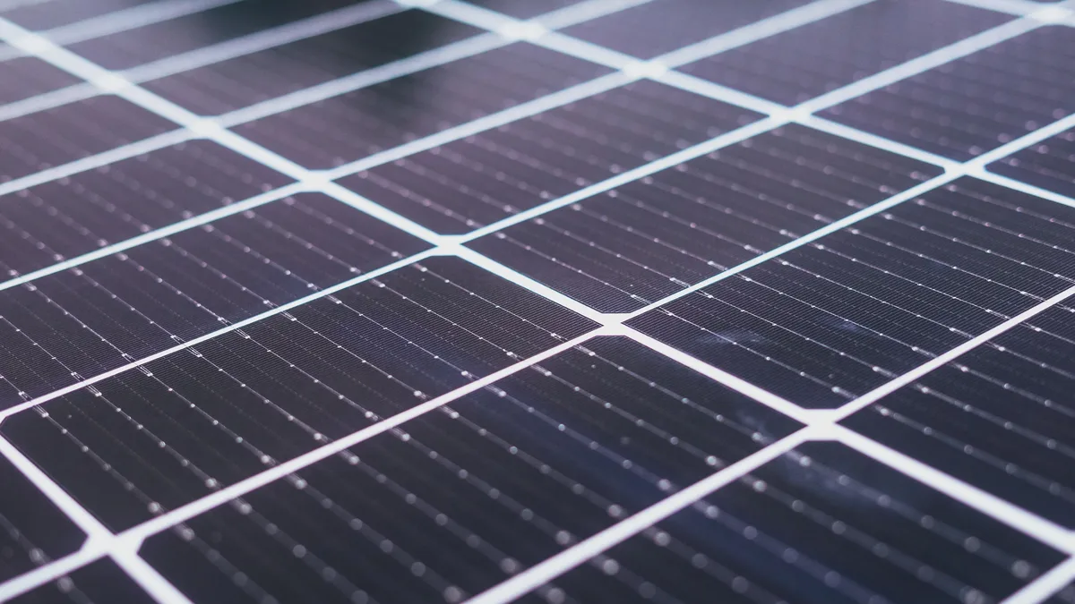
A back contact cell is a type of silicon solar cell where both the positive and negative electrical contacts are located on the rear surface of the device. This architectural shift fundamentally differs from conventional cells that have a grid of metal fingers and busbars on the sun-facing side. The most prevalent commercial design is the interdigitated back contact (IBC) cell, which features alternating bands of n-type and p-type semiconductor material and their corresponding metal contacts on the back in an interlocking pattern. This requires extremely precise manufacturing to align the doped regions with their respective contact fingers without any front-side metallization. High-quality, low-defect silicon substrates, typically n-type monocrystalline silicon, are used to ensure long minority carrier lifetimes necessary for carriers to travel from the front to the rear contacts. The complete absence of metal on the front is often complemented by advanced surface passivation and light-trapping schemes to further boost performance.
What to know
The manufacturing process for back contact cells is notably more complex and capital-intensive than for standard cells, involving additional photolithography or laser patterning steps. This complexity historically resulted in a significant cost premium, though manufacturing innovations continue to narrow this gap. The cells require specialized module assembly techniques, as the electrical interconnections must be made only from the back, often using conductive adhesives or soldering to a complex rear-side circuit. Performance-wise, they typically exhibit a higher temperature coefficient than some other premium technologies, meaning their efficiency advantage can diminish slightly more in very hot operating environments. The homogeneous black appearance is a key selling point, but it can sometimes lead to slightly higher cell temperatures due to lower light reflection. It is crucial to understand that the term "back contact" describes an architecture, not a single technology, with variations like IBC, metal wrap through (MWT), and emitter wrap through (EWT) having different performance and manufacturing characteristics.
Common questions
Are back contact modules more efficient than standard panels? Yes, commercially available back contact modules consistently rank among the highest in efficiency for mass-produced silicon photovoltaic products. How does the electricity get to the back if the contacts are only there? Light-generated electrons and holes travel through the entire thickness of the silicon wafer to the respective n and p contacts on the rear, which requires very high-quality silicon material. Do they work on cloudy days or with indirect light? They generate electricity under diffuse light conditions like all solar cells, but their primary advantage in reduced shading loss is most pronounced under direct sunlight. Are they more fragile or difficult to install? The cells themselves can be more fragile due to their specific structure, but they are laminated into standard module formats, so installation procedures are generally the same. Why are they often more expensive? The higher cost stems from complex cell fabrication, the use of premium n-type silicon, and specialized interconnection materials within the module. Can they be used with solar trackers? Yes, they are well-suited for tracker systems, where their high efficiency and uniform response can maximize energy harvest throughout the day.
Pros and cons
Pros: The foremost advantage is the highest commercially available conversion efficiency for silicon PV, leading to greater power output per unit area. The elimination of front metallization removes a permanent source of optical loss, allowing more light into the cell. This also results in a uniform, all-black aesthetic that is highly valued in residential and architectural markets. The rear contact design can reduce series resistance losses by allowing for wider, optimized contact grids. It also avoids potential issues with front-contact corrosion over the module's lifetime. The architecture minimizes current-induced degradation effects common in some p-type cells, contributing to long-term performance stability. Cons: The principal disadvantage is higher manufacturing cost due to complex processing steps like precise doping alignment and rear-side patterning. The reliance on high-purity n-type silicon wafers makes the cell cost more sensitive to upstream material pricing. The common mistake is selecting this technology for cost-sensitive projects where the efficiency premium cannot justify the initial capital expenditure, leading to regret over not achieving a lower levelized cost of energy. They can exhibit a marginally higher temperature coefficient, meaning in extremely hot climates, some of their peak efficiency advantage may be reduced compared to technologies with a lower coefficient. The specialized interconnection process can also pose challenges for module repairability in the field.
Who it suits
This technology suits project developers and homeowners with space constraints who need to maximize energy production from a limited roof or land area. It is well-matched for residential customers who prioritize aesthetics and are willing to pay a premium for a sleek, uniform black appearance that integrates seamlessly with roofing materials. Commercial and public projects with a focus on sustainability branding or architectural design often select back contact modules for their high performance and visual appeal. It is suitable for manufacturers and investors focused on the high-efficiency segment of the market, competing on performance rather than lowest cost per watt. The technology is less suited for large-scale utility projects where the lowest upfront cost is the primary driver and vast land area is available, making absolute efficiency less critical than overall system cost.
Latest Back Contact Cells news
Latest reporting
India's Solar Manufacturing Surge Faces Cell Supply
India added 50.6GW of solar module and 9.7GW of cell capacity in H1 2026, but a critical shortage of domestic cells is slowing production and project
Sungrow to use Samsung SDI battery cells for US energy
Sungrow plans to procure lithium iron phosphate battery cells from Samsung SDI for its energy storage systems, primarily to support its U.S.

CATL and EVE Energy lead battery storage
Major Chinese battery manufacturers, led by CATL and EVE Energy, are raising prices for energy storage cells, driven by a new consumption tax and...
European PV Module Prices Decline in August 2026
European PV module prices fell in August 2026 as demand dipped below historic averages, with back contact, full black, and monofacial TOPCon modules
CATL Cuts LFP Battery Prices Amid Industry Shifts
CATL has cut prices for its 314Ah lithium iron phosphate cells, a move analyzed by industry experts. The broader energy storage sector also saw...
China urged to back local solar finance in Global South
Analysts say China, the world's top solar equipment exporter, should help catalyze local capital for off-grid solar projects in the Global South...