Gray vs. Blue wafer distinction critical for U.S. Solar
The technical difference between unprocessed gray wafers and partially finished blue wafers is central to accurately assessing domestic manufacturing depth
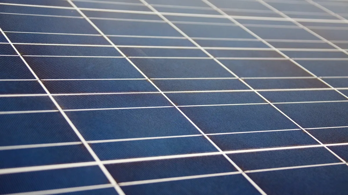
A gray wafer is an unprocessed silicon wafer that cannot generate electricity on its own. A blue wafer has its P/N junction already formed and typically includes an anti-reflective coating, giving it the core semiconductor structure needed for photovoltaic conversion.
Turning a gray wafer into a functioning solar cell requires a sequence of processes. These include texturing, cleaning, junction formation, edge isolation, passivation, anti-reflective coating application, metallization, and testing. The formation of the photovoltaic junction is a significant step. It is achieved by introducing a layer of opposite conductivity type to the crystalline-silicon wafer, either through high-temperature dopant diffusion or deposition of doped semiconductor layers. This junction creates the electric field that allows the device to separate charge carriers and convert sunlight into electricity.
A blue wafer has undergone this junction formation by the time it reaches a factory. It has also typically received the anti-reflective coating that gives it a blue appearance. While metallization and other finishing processes may still be required, the blue wafer already possesses the fundamental semiconductor structure that enables photovoltaic conversion.
Why junction formation determines domestic content
In solar trade proceedings, the location where the P/N junction is formed has historically been an important factor in determining a solar cell’s origin. For solar cells, that requires examining the manufacturing sequence and determining where a silicon wafer acquires the characteristics that make it a photovoltaic device. This reflects the technical significance of junction formation in creating a device capable of photovoltaic conversion.
How incomplete documentation risks compliance and incentives
Different regulatory frameworks may define 'domestic' differently. Domestic content calculations examine where specific manufactured products and components are produced. Customs and trade authorities may apply separate standards when determining a product’s country of origin. Module manufacturers rely on cell suppliers’ representations to determine product origin and calculate domestic content levels. Developers use this information to model project economics and support eligibility for federal incentives. Tax-credit investors, lenders, and insurers evaluate the same documentation as part of project diligence.
If the underlying manufacturing process has been inaccurately described, consequences may include challenged domestic content calculations, reduced expected incentives, and disputes over pricing or responsibility. Not every product involving imported blue wafers is necessarily noncompliant. Treatment depends on applicable law, the specific production process, and transaction facts. Buyers should understand precisely what they are purchasing and avoid treating all U.S.-finished cells as technically or legally equivalent.
A credible chain of documentation should identify the material entering the U.S. Facility, where the P/N junction was formed, and which manufacturing processes were performed domestically. Useful diligence questions should become part of routine procurement. Clear documentation protects responsible manufacturers while giving customers greater confidence in their sourcing and incentive calculations.
What responsible sourcing and policy should require
A facility that imports gray wafers and performs critical cell-making processes domestically carries out a different scope of manufacturing than a facility that imports blue wafers and completes only downstream steps. Both operations require equipment, workers, and quality controls. They do not necessarily represent the same level of technical transformation, manufacturing value, or domestic capability.
Policymakers are evaluating whether federal incentives are supporting the development of an enduring U.S. Solar manufacturing base. Incentives designed to encourage domestic solar cell production are most effective when they support the processes, equipment, and expertise required to transform a gray wafer into a functioning cell. If nearly completed cells can enter the country as wafers and receive the same treatment, the market may reward finishing operations the same way it rewards more comprehensive manufacturing. Over time, that could weaken the incentive to invest in the full range of domestic capabilities.
Effective policy must recognize where meaningful technical transformations occur, not only the factory address. The industry should not rely on a single broad claim, such as 'U.S.-made,' as a substitute for a process-specific compliance analysis. The relevant question is which manufacturing steps occurred in each country and how those steps are treated under the particular rule being applied. Clear, consistently applied definitions would benefit manufacturers, buyers, developers, and policymakers.
As the market matures, traceability will become as important as production capacity. Achieving a solar manufacturing base grounded in technical depth requires looking beyond where a product is finished and asking where the wafer actually became a solar cell. Industry stakeholders should adopt routine procurement practices that document where the P/N junction was formed and which processes occurred domestically.